Welcome, and thank you for reading things!

| Panel | ||
|---|---|---|
| ||
Welcome! The following document will help you understand how the formatting of your design project affects the automated processes provided to you. |
PCB Formatting FAQs
What design formats are supported?
ODB ++ and Gerber formats are supported.
Additional files in the project collection are ok to include as long as the design files are in one of the above mentioned formats.
Where do I get those formats?
Export from your favorite eCAD design program (Native eCAD files are not supported)
How should I name the files so they can be read automatically?
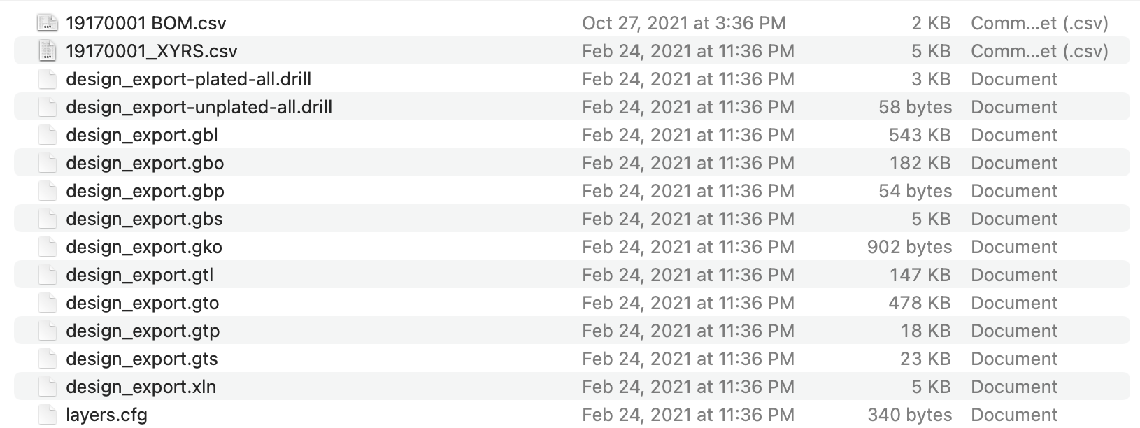
Gerber file names must follow a reasonable naming convention - either the file name should include the layer type (e.g. top_silk, bottom_copper, etc.), or you can use commonly recognized file extensions
Example
How should the project be packaged?
For Gerber files, you can provide:
A zip OR
Multi-select and drop all of the individual files
ODB++ projects must be in a compressed file, typically .tgz
What does a bad package look like?
Incorrect file formats (remember ODB++ and Gerber project files)
Packages which contain many revisions of the same project (pick the ONE you want to process)
“Just give me an example!”
Sample project and sample BOM:
| View file | ||
|---|---|---|
|
| View file | ||
|---|---|---|
|
BOM Formatting FAQs
How can I get an estimate on a PCB assembly?
It’s easy. Simply include a Bill Of Material (BOM) with your project and you will receive a pricing estimate for a complete assembly (if your selected supplier provides assembly services).
What file formats are accepted?
You can upload an xls, xlsx or csv file (only the first sheet of a spreadsheet will be processed)
How can the PCBQuickPrice tool find my part numbers in a spreadsheet?
BOM files must be formatted with reasonable column header names to identify the information automatically.
Example of a well formatted BOM:
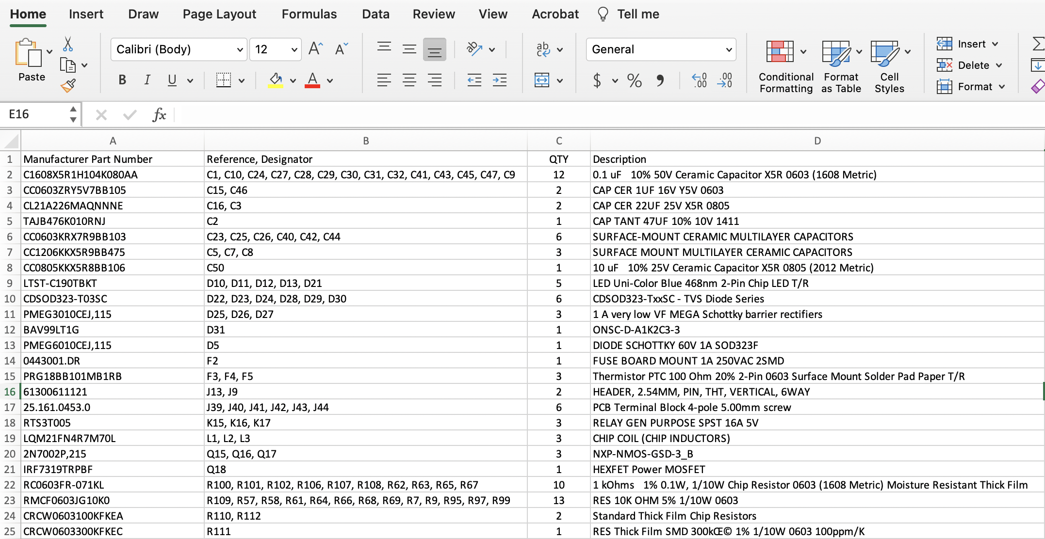
Can I use my internal reference part numbers?
To check pricing and availability we need the manufacturer’s part number. We can provide an estimate on labor with internal part numbers but not total BOM cost.
Example Project
You can download a good example of a project to see how the files are named, review the BOM formatting, and use it to test the PCBQuickPrice tool.
| View file | ||
|---|---|---|
|
| View file | ||
|---|---|---|
|
| View file | ||
|---|---|---|
|
It’s not working, I’m not getting a price. - Troubleshooting
The most common reason that users don’t receive a price automatically is due to the name of the Gerber files. If there are no identifiable names or extensions, the layers can not be assigned automatically and a price can not be calculated. Make sure to check both the file names and extensions of your Gerber files.
The second most common problem is duplicate projects in a single zip file. Make sure there are no old revisions or panel files in one of the subfolders
Check if your BOM file has “BOM” in the file name
Make sure your part numbers are on the first sheet with a reasonable header name - you’d be surprised how often it ends up on the second sheet in a spreadsheet
A layer limit of 8 is in place for automated pricing. The tool will help you engage to get pricing outside of that scope.
It’s possible that your board contains features/attributes that your selected supplier does not support for automatic pricing (e.g. too large for a standard panel) - fill out the form to contact the supplier and confirm whether your project is a good fit.
Automated Pricing Defaults
The PCBQuickPrice pricing is based on the below default options. Don’t worry; as you engage further you can specify alternative preferences for more accurate prices. This is just a ballpark to help you budget and make decisions.
Green Soldermask
White Silkscreen
1 oz copper
HASL-LF finish
FR-4 material
No controlled impedance
These setting cannot be changed
PCB Layers
PCBs can be manufactured with one to many layers. The most common designs are typically between 2 and 8 layers with an even number of layers.
Layer pricing is calculated using an even number of layers, so a 7 layer board costs the same as an 8 layer board.
Boards with more than 8 layers are difficult to price automatically due to non-standard stocked material and may require a manual quote.
Boards with more than 8 layers are typically more expensive, so if possible, design your product with a more standard layer count (2, 4, 6, 8 layers).
PCB Board Size
A single PCB can be almost any size, limited only by the panel size of the manufacturer.
Typically manufacturers use a standard panel size of approximately 450 x 600 mm [18 x 24 in]
Other panel sizes are available but may require a custom quote.